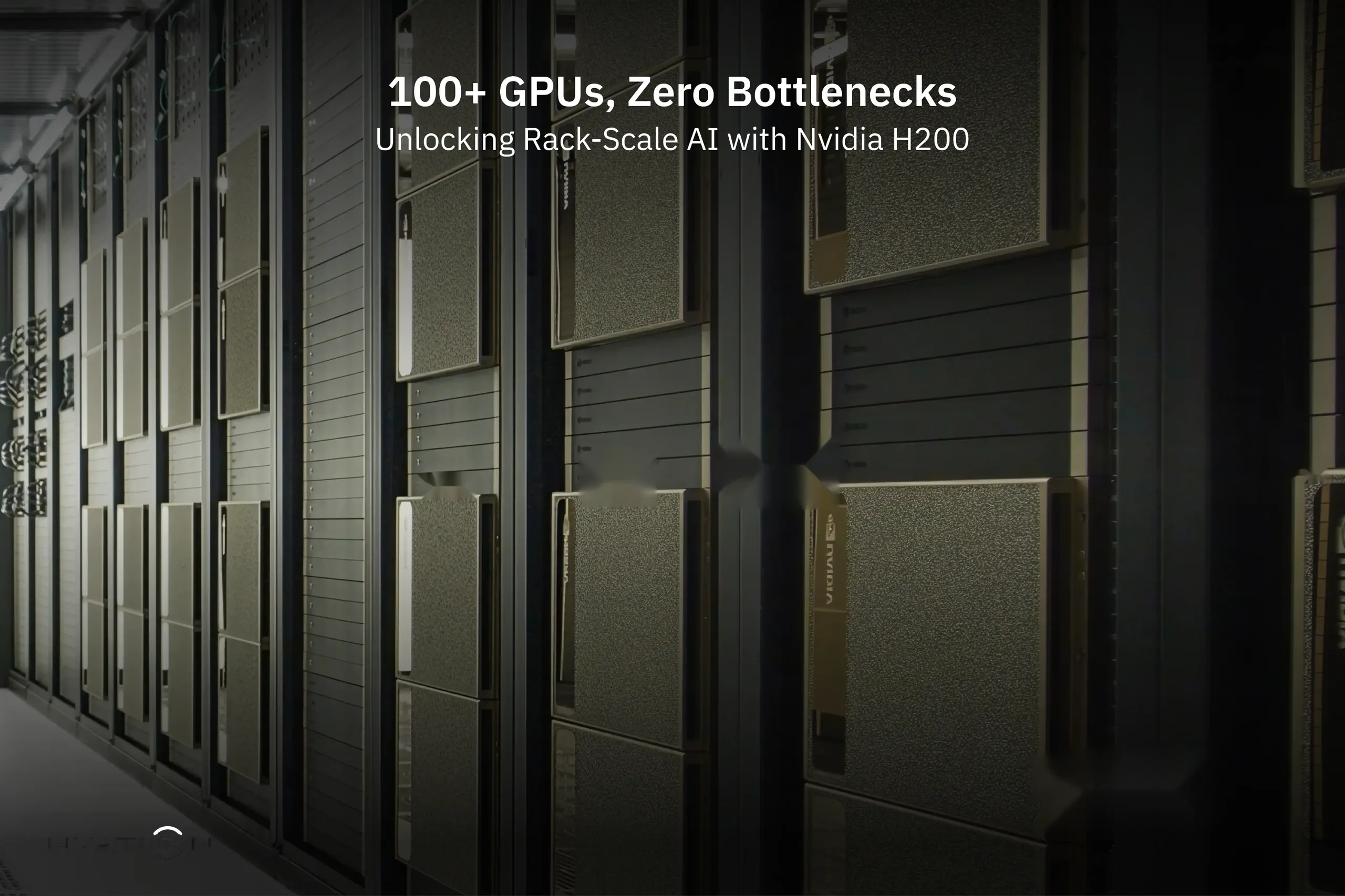
FEATURED STORY OF THE WEEK
NVIDIA H200 and NVLink Bridges: Unlocking Next-Gen GPU Scaling for AI and HPC
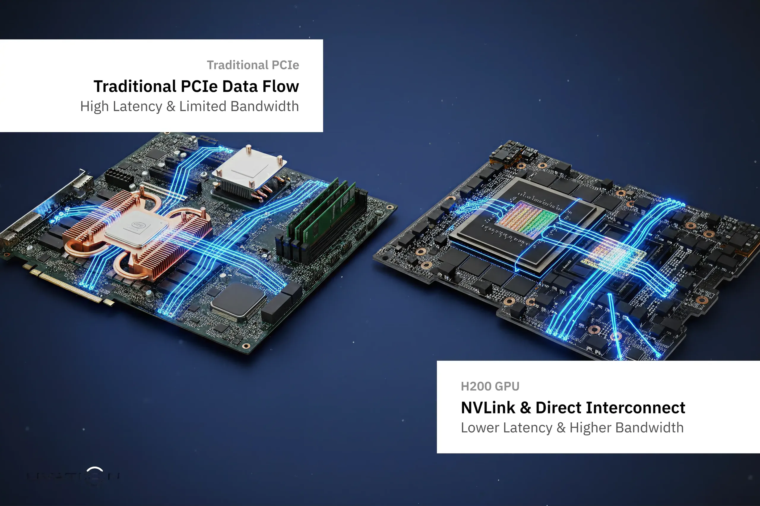
n modern AI and HPC environments, performance is no longer defined by GPU count alone. Many enterprises discover that adding more GPUs doesn’t automatically translate into faster model training or better inference throughput. The real challenge lies in how these GPUs communicate. When thousands of operations per second depend on data moving fluidly between processors, even small interconnect bottlenecks can stall entire workloads. This is where NVIDIA’s H200 GPU and NVLink Bridges come together, forming a high-speed data pathway that allows multiple GPUs to work as a synchronized unit.
The NVIDIA H200, part of the Hopper architecture, brings exceptional processing performance supported by NVLink, a high-bandwidth interconnect designed to accelerate GPU-to-GPU communication. NVLink Bridges act as the physical link between GPUs, enabling them to share memory and exchange data at speeds far beyond PCIe standards. Together, they create a tightly coupled compute environment suited for AI training, simulation, and large-scale inference.
This blog will examine how the NVIDIA H200 and NVLink Bridges function as a unified architecture, the design trade-offs involved, and the engineering practices that help data center architects and IT leaders build efficient, high-performance GPU infrastructures.
1. Architecture of the NVIDIA H200: What’s New
The NVIDIA H200 GPU represents a major architectural step within the Hopper family, advancing how enterprises train and deploy large AI and HPC workloads. It focuses on faster data access, stronger inter-GPU communication, and improved efficiency for memory-intensive operations such as generative AI inference and scientific simulation.
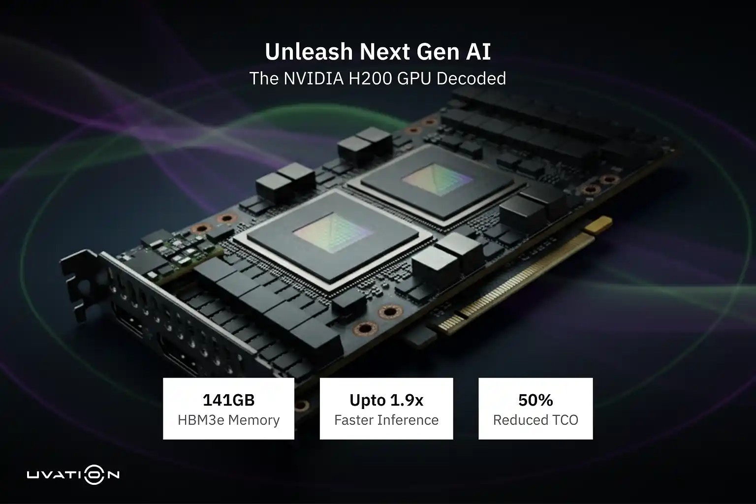
H200 Key Specs and Positioning
The NVIDIA H200 builds on the Hopper architecture introduced with the H100, designed to handle massive parallel workloads typical of foundation models and data-intensive computation. The H200 is the first GPU to feature HBM3e memory, offering up to 141 GB of capacity and 4.8 TB/s of memory bandwidth, which significantly reduces memory bottlenecks during model training and inference.
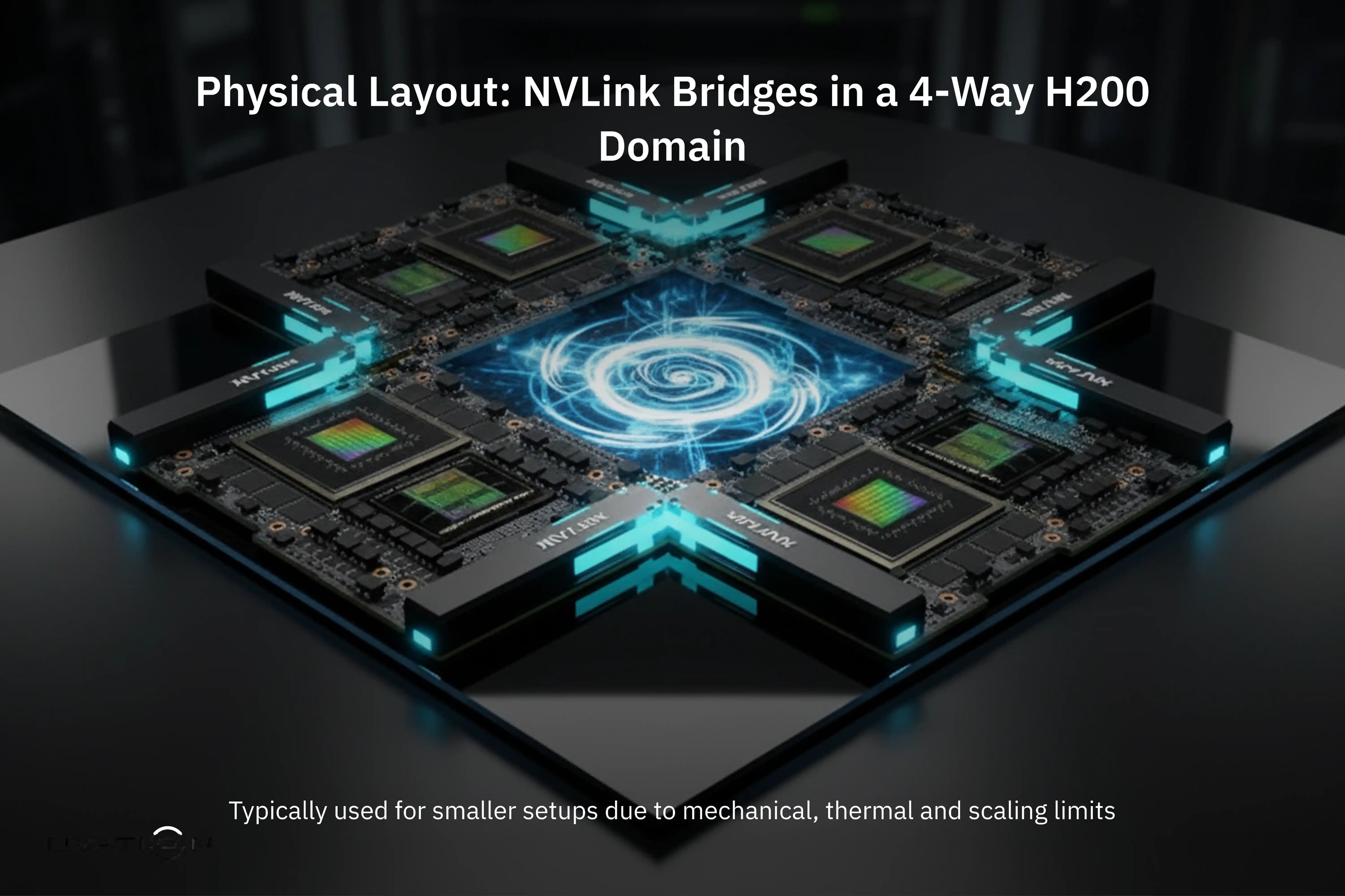
This GPU supports a 4-way NVLink interconnect domain, enabling direct, high-bandwidth communication between up to four GPUs. The combined bandwidth reaches 1.8 TB/s, allowing data to move fluidly between processors without routing through the CPU or system memory. This design is particularly valuable for workloads that demand synchronized GPU cooperation, such as large language model inference and AI simulation.
The H200 also offers improved energy efficiency and enhanced compute throughput over the H100, driven by its refined Tensor Core design and increased memory bandwidth. In practice, this means faster training convergence and reduced inference latency for high-performance workloads.
NVLink Integration in H200
At the heart of the H200’s performance is NVLink, NVIDIA’s high-speed interconnect that replaces traditional PCIe bottlenecks in multi-GPU configurations, leveraging the NVLink protocol for optimized GPU-to-GPU communication. The H200 includes multiple NVLink channels, creating a 4-way full mesh that allows each GPU to communicate directly with every other GPU in the domain. This reduces latency and improves data-sharing efficiency, ensuring that complex models can span multiple GPUs without performance degradation.
For data center environments, NVIDIA offers an H200 NVL variant. This version is designed for rack-level scale-out configurations, allowing GPUs to be connected across server boards within a cluster. NVLink in these systems functions as a unified data fabric, delivering consistent bandwidth and latency across multiple nodes.
Implications for Scale: Memory, Latency, and Coherence
The introduction of HBM3e memory and NVLink connectivity changes how systems handle large-scale models. The NVLink protocol enables GPUs to share memory regions and perform peer-to-peer transfers at speeds many times faster than PCIe connections. It can improve inter-GPU communication throughput dramatically compared to PCIe Gen5, significantly reducing the time spent on data exchange.
However, achieving consistent performance across NVLink-connected GPUs requires software awareness. Frameworks such as PyTorch, TensorFlow, and NVIDIA’s NCCL (NVIDIA Collective Communication Library) must be configured to understand the NVLink topology. This ensures that GPU tasks are routed efficiently across direct links, avoiding unnecessary hops that can introduce latency.
2. NVLink Fundamentals and Evolution
Understanding NVLink is essential for anyone designing or deploying modern GPU-based infrastructure. It is the communication backbone that connects multiple GPUs into a coherent, high-bandwidth compute fabric.
What Is NVLink?
NVLink was introduced by NVIDIA as a high-speed interconnect to enable direct GPU-to-GPU communication. Traditional PCIe links limited data exchange between GPUs, causing performance bottlenecks during parallel training and inference. NVLink addresses this by providing dedicated high-bandwidth, low-latency connections between devices.
Over time, NVLink has evolved to support higher link counts, faster signaling rates, and wider connectivity. Each generation of NVLink builds upon the previous one to support growing data workloads and GPU clustering requirements.
NVLink Bridges and Bridge Architecture
An NVLink Bridge is a compact hardware connector that physically links two GPUs together, forming an NVLink mesh. It enables direct peer-to-peer communication without routing data through the motherboard or system memory. Bridges are particularly common in workstation and server configurations where GPUs are mounted on PCIe boards rather than integrated into a backplane.
Earlier GPU generations, such as NVIDIA Quadro RTX and TITAN RTX, relied on NVLink Bridges to deliver shared memory and unified workloads across two GPUs. Bridge models varied in slot spacing—for example, 2-slot and 3-slot variants—to accommodate different GPU form factors. Some high-end systems used active bridges with signal conditioning circuits for long connections, while simpler setups used passive bridges. NVIDIA specifies bridge compatibility for each GPU model to maintain performance and electrical stability.
However, bridges are not without limitations. Factors such as signal integrity, thermal constraints, and mechanical stress must be considered during installation. Improper spacing or airflow restriction can degrade performance or reduce component lifespan. For large GPU clusters, bridge-based designs eventually reach a scaling limit, prompting NVIDIA to develop more advanced solutions like NVLink Switch.
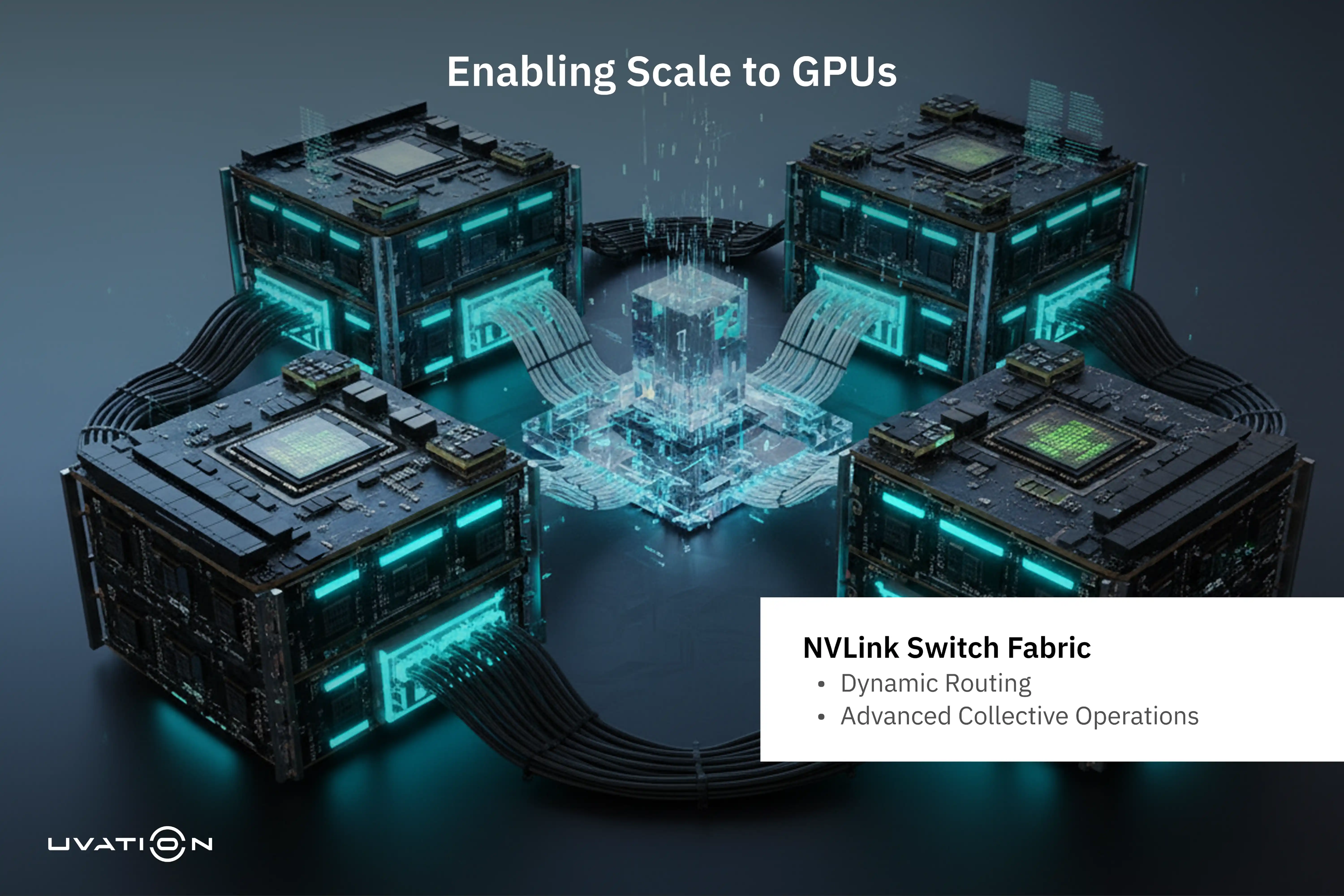
NVLink Switch and NVLink Fusion
As GPU deployments expanded from a few GPUs per node to dozens per rack, point-to-point bridge connections became impractical. NVIDIA addressed this by introducing NVLink Switch technology, which connects multiple GPUs through a switching fabric rather than direct physical links. This approach allows for multi-node GPU clusters with consistent low-latency communication across the entire system.
The NVLink Switch also supports advanced operations such as aggregation and in-network reduction, which minimize communication overhead during collective GPU operations. These features are vital for workloads involving distributed training or large-scale simulation.
Building on this foundation, NVLink Fusion extends NVLink’s capabilities to connect different types of processors, including CPUs, GPUs, and specialized accelerators. This creates a direct chip-to-chip communication layer across heterogeneous components—an important step for systems like NVIDIA Grace Hopper, where CPUs and GPUs operate in tight synchronization. Through these evolutions, NVLink has matured from a simple GPU bridge into a high-speed, system-wide interconnect architecture.
3. Mapping NVLink Bridges to H200 Deployments
As NVIDIA H200 GPUs find their place in enterprise AI infrastructure, understanding how NVLink Bridges, or their internal equivalents, operate within these deployments becomes essential. The physical and logical interconnect design directly influences memory sharing, communication speed, and ultimately, model training efficiency.
How NVLink Bridges (or Equivalent Interconnects) Are Used with H200
In NVIDIA DGX and HGX systems featuring H200 GPUs, inter-GPU communication is typically achieved through internal NVLink routing rather than external bridge modules. These server-class configurations use dedicated NVSwitch chips to create high-bandwidth, low-latency GPU meshes inside the chassis. According to NVIDIA’s Hopper architecture documentation, each H200 supports up to 18 NVLink connections, enabling an aggregate bandwidth of up to 1.8 TB/s across four GPUs within a single domain.
For PCIe-based or workstation implementations—which are less common for the H200 class—NVLink Bridges can still be relevant. These physical bridge modules connect GPUs directly, enabling shared memory access and faster data movement compared to PCIe-only setups.
Bandwidth and Latency Expectations
Each H200 GPU offers up to 1.8 TB/s aggregate NVLink bandwidth when configured in a 4-way NVLink domain. This figure represents total bidirectional capacity; individual GPU pairs see portions of this bandwidth depending on link configuration.
In practical workloads, NVLink provides substantially lower latency compared to PCIe, reducing GPU-to-GPU communication delays by several orders of magnitude. However, scaling efficiency decreases when workloads span across many GPUs without NVLink-aware optimization. Software frameworks must coordinate communication patterns carefully to prevent bottlenecks from emerging in model synchronization or data exchange.
Programming and Software Implications
To fully exploit NVLink interconnects, developers must use topology-aware programming frameworks such as NCCL (NVIDIA Collective Communication Library) and NVML (NVIDIA Management Library). These tools allow precise mapping of communication paths and monitoring of interconnect performance. Utilities like nvidia-smi topo can display the GPU topology, helping developers identify optimal GPU pairing and reduce unnecessary data hops.
Incorrect topology mapping or naïve “all-reduce” operations across distant GPU pairs can lead to extra latency and reduced efficiency. Continuous monitoring of NVLink link status, bandwidth utilization, and error counters is equally important, ensuring that GPU communication remains healthy and consistent across workloads.
4. Comparative Table: Bridge-based vs Switch-based NVLink in H200 Systems
| Aspect / Metric | Bridge-Based | Switch / NVLink Switch / Fusion |
|---|---|---|
| Scalability | Works well up to 4–8 GPUs | Scales to dozens or 100+ GPUs |
| Latency / hops | Minimal (direct) | May incur internal switch latency |
| Complexity of wiring | High manual cabling | Simpler when using backplanes or switch chips |
| Fault isolation | Local – link drop affects two GPUs | Switch failure may impact many GPUs |
| Flexibility | Rigid (fixed pairing) | Dynamic routing & aggregation support |
| Ideal use case | High-performance 4-GPU clusters | AI factories, rack-scale clusters |
5. Deployment Guidelines and Best Practices
Deploying NVIDIA H200 GPUs with NVLink Bridges or equivalent interconnects demands careful system planning. Every detail—from board spacing to software topology mapping—affects overall throughput and stability. The following guidelines outline the key engineering and operational considerations for designing, validating, and maintaining NVLink-based GPU environments.
Planning the GPU Layout and Board Spacing
Correct board spacing is the foundation of a reliable NVLink configuration. Bridge modules have strict mechanical pitch requirements—typically determined by the GPU board’s slot spacing. If boards are installed too close or too far apart, the bridge cannot seat properly, leading to poor electrical contact or physical strain.
Adequate airflow is equally important. NVLink Bridges can obstruct airflow paths between GPUs, especially in dense workstation or rack-mount systems. Designers should allocate thermal headroom for each GPU and confirm that bridge placement does not impede cooling. For longer trace lengths or environments with high electrical noise, active bridges—which include built-in signal conditioning—are recommended to maintain signal quality and data reliability.
Thermal, Power, and Signal Integrity
NVLink hardware operates at extremely high frequencies. Even small impedance mismatches or temperature fluctuations can degrade signal integrity. During design validation, engineers should check differential pair matching, impedance control, and return loss parameters to ensure consistent communication between GPUs.
From a thermal perspective, bridges contribute to the overall heat density around the GPU socket. NVIDIA recommends maintaining thermal margins and ensuring the bridge modules are within the rated temperature envelope for sustained workloads. Power delivery should also be validated to avoid voltage droop during peak inter-GPU communication bursts.
Error Handling, Link Repair, and Redundancy
NVLink communication errors can stem from hardware wear, connector degradation, or firmware instability. Engineers should monitor error counters through the NVIDIA Management Library (NVML) or driver logs, focusing on ECC (Error Correcting Code) and CRC (Cyclic Redundancy Check) metrics. Early detection allows proactive maintenance before failures affect workloads.
In large-scale configurations, designing for redundancy is advisable. Including spare NVLink paths or additional GPUs allows systems to maintain communication even if one link fails. Some NVSwitch-based systems also support automatic rerouting, which can sustain performance under partial link degradation.
Conclusion
The NVIDIA H200 represents a major step forward in GPU-based computing, pairing massive compute density with advanced interconnect design. Its built-in NVLink capability delivers up to 1.8 TB/s of aggregate inter-GPU bandwidth, far exceeding PCIe performance. This high-speed fabric allows GPUs to share memory, exchange tensors, and synchronize gradients at a rate suited for today’s large-scale AI and HPC models.
In workstation or smaller server configurations, NVLink Bridges provide the essential physical pathway for GPU-to-GPU coherence. In contrast, rack-scale deployments rely on internal NVLink routing or NVLink Switch fabrics, allowing multi-node systems to maintain similar low-latency communication at greater scale.
Ultimately, achieving peak efficiency with the NVIDIA H200 requires more than hardware alone. Engineers must carefully design the interconnect topology while tuning software frameworks to match these physical pathways. When executed correctly, the synergy between H200 GPUs and NVLink infrastructure transforms communication overhead into parallel throughput, setting a new performance baseline for enterprise AI clusters and advanced scientific computing platforms.
More Similar Insights and Thought leadership
No Similar Insights Found
Subscribe today to receive more valuable knowledge directly into your inbox
We are writing frequenly. Don’t miss that.
Subscribe to get updates

Unregistered User
It seems you are not registered on this platform. Sign up in order to submit a comment.
Sign up now